Many S-100 users
have some kind of ASCII style parallel port keyboard attached to their
system. The interface was just a simple 8 bit parallel input port with
a second port single strobe bit. Most of these keyboards came from old
mini computer systems or simple CRT terminals. Today they are now quite difficult to
find. If there are any parallel port keyboards on eBAY etc. from Atari
systems and the like, they are usually not in ASCII format but instead
deliver key press data in X,Y coordinates etc. Today almost all PC
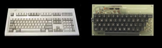
systems interface the user via an IBM PC (AT) type keyboard. This is in fact
may be the single most lasting effect the IBM PC has had on the PC business in
the past 30 years.
However the IBM keyboard does not return data to the computer via a parallel
port. Instead it does so in a more sophisticated manner via a bidirectional
serial communication mode. Each key returns its own (single or
multiple 8 bit code) which is different on the key down and up strokes. It
also depends on the status of the Ctrl, Num, Alt and other keys. To make matters worse IBM took two
try's at
the process. The original IBM-PC started with a more simpler serial data
format that actually worked fine. However (just when clones of these
keyboards started to appear) IBM came out with a second more complex serial
communication protocol for their Keyboard in their IBM-PC AT. This
protocol is what almost every PC-style keyboard uses today.
There are still some of the old PC and XT keyboards. They will not
work on modern systems (or with the board described below).
The Keyboard Serial Communication Protocol.
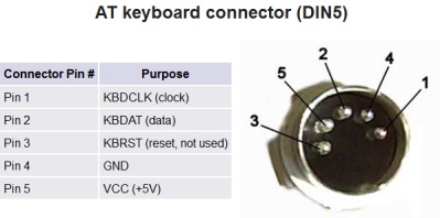
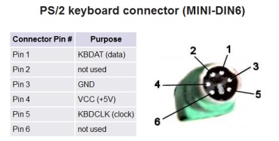
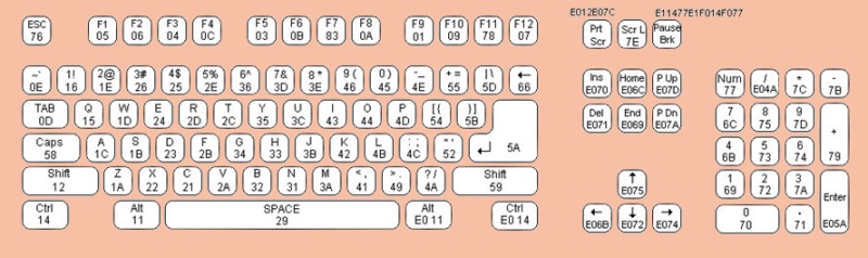
There are actually two types of sockets used for these IBM type keyboards
(not counting the newer USB port driven ones). The original socket was the
larger AT style socket shown below. The much more common socket today
is the PS/2 style socket. (Perhaps the only contribution/residual of the
ill famed IBM PS/2 computer). The pinouts are different. The view shown is
that of looking into the male socket of the keyboard cable itself.
In all cases communication between the computer and keyboard is
bidirectional over only two data lines. A "Clock Line" and a "Data Line".
Both data lines are Open Collector TTL signals. Let us look at
communications in each direction separately.
Keyboard to Computer. At any time the Computer has the ultimate priority over direction. It can at
anytime send a command to the keyboard. That said, the keyboard
is free to send data to the Computer when both the Keyboard Data and
Keyboard Clock lines are high (Idle). The Keyboard Clock line can be used
as a sort of Clear to Send line. If the Computer takes the Keyboard Clock
line low, the keyboard will buffer any data until the Keyboard Clock is
released, i.e. goes high. Should the Computer take the Keyboard Data line low,
then the keyboard will prepare to accept a command from the Computer.
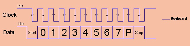
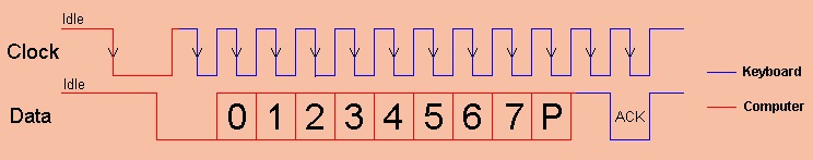
The transmission of data in the forward direction, i.e. Keyboard to
Computer, is done with a serial frame of 11 bits. The first bit is a Start Bit
(Logic 0) followed by 8 data bits (LSB First), one Parity Bit (Odd Parity)
and a Stop Bit (Logic 1). Each bit should be read on the falling edge of the
clock.
The above waveform represents a one byte transmission from the Keyboard. The
keyboard may in fact not actually change it's data line on the
rising edge of the clock as shown in the diagram, the data line only has to
be valid on the falling edge of the clock. The
Keyboard will generate the clock. The frequency of the clock signal
typically ranges from 20 to 30 KHz on most systems. Note in particular in
this protocol the Least Significant Bit is always sent first.
Computer to Keyboard
The Computer to Keyboard Protocol is initiated by taking the Keyboard data
line low. However to prevent the keyboard from sending data at the same time
that you attempt to send the keyboard data, it is common to take the
Keyboard Clock line low for more than 60us. This is more than one bit
length. Then the Keyboard data line is taken low, while the Keyboard clock
line is released. The keyboard will start generating a clock signal on it's Keyboard clock
line. This process can take up to 10mS. After the first falling edge has
been detected, you can load the first data bit on the Keyboard Data line.
This bit will be read into the keyboard on the next falling edge, after
which you can place the next bit of data. This process is repeated for the 8
data bits.
After the data bits come an Odd Parity Bit.
Once the Parity Bit has been sent and the Keyboard Data Line is in a idle
(High) state for the next clock cycle, the keyboard will acknowledge the
reception of the new data. The keyboard does this by taking the Keyboard
Data line low for the next clock transition. If the Keyboard Data line is
not idle after the 10th bit (Start, 8 Data bits + Parity), the keyboard will
continue to send a Keyboard Clock.
All this to save one extra wire on a keyboard cable! An extra wire
(directional flow etc) could make things so much easier to emulate. Anyway
this is what we have to work with. An S-100 Board to accept an
IBM PC keyboard input.
In order to use the above keyboard format in a S-100 system we have a bit of
a challenge. Not only is the data is a serial format, but the actual
format itself is not one that could be spliced into a standard UART chip.
We need to emulate exactly what a PC computer reads. Now
fortunately for us the only significant communications going from the
computer to the keyboard are signals to turn
on/off the caps lock, shift etc LEDs on the keyboard. All other
communication is from the
keyboard to the computer.
We'll address the LED's issue later. The complication we have is that
the actual keyboard key codes (scan codes as they are called), sent from each
key is somewhat complex and depends on whether the Shift, Ctrl, Alt, Number
Lock of Function keys are pressed. To make matters worse in some
case pressing one key generates code to for more than a single scan
code. Also every UP key is the same as its DOWN key code except it is
preceded by a 0F0H scan code. The figure below shows a simplified diagram of
the key DOWN key
scan codes.
Over the years many have tackled this challenge in various ways to hammer
an ASCII code out of these keyboards. Some use elegant single chip
CPU/IO chips (PIC etc.), others various TTL logic chips. I decide to tackle the
problem head on by using the age old Z80 CPU, RAM/ROM and a few Zilog PIO's.
This not only allows one to completely control the data sent from each and
every key combination simply (lookup tables), but the keys can be dynamic,
function keys can return varying strings depending on the application.
I chose the Z80 because almost everybody in the S-100 bus world knows the
opcodes and can easily program a simple common 2716 EPROM or the like, for their own
specific applications/desires.
Years ago back in 1986 I wrote up an article for Sol Lib's Micro/Systems
Journal about a simple Z80 based board to convert the original IBM-PC scan
codes to an
ASCII parallel port keyboard format. This article can be seen
here. This board
worked for the earlier first generation PC keyboards mentioned above.
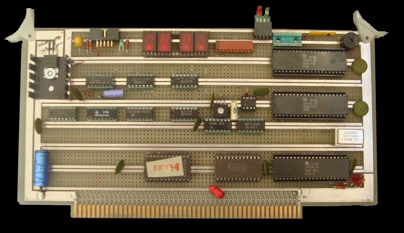
This new S-100 board is an extension of that board with more bells and
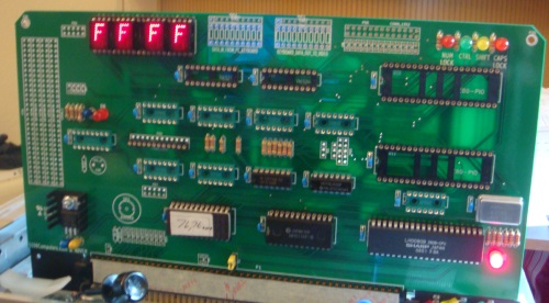
whistles. Here is a picture of the S100 prototype board.
The board is really a small microcomputer system with its own RAM, ROM and
I/O ports. Its only function in life is to watch the data coming in
from the keyboard and translate each key scan code into an ASCII letter or
string. While this process could probably be done by carefully
watching a one bit data and clock input with careful timing. It is just
easier to shift the serial data into 2+2 74LS164 serial to parallel IC chips.
A detailed schematic is shown
here (Thanks
to the hard work of Andrew Lynch, see below).
IC3A and 4A (74LS164's) collect the serial data bits and send them back to the Z80 (via PIO #1)
as
8 raw data bits. IC1A and 2A simply count the clock bits.
Stopping further shifting when 11 clock pulses have been received and
sending a strobe to the Z80 (pin 5 of IC1A to PIO #1 pin 27).
The Z80 then reads the scan code and via lookup tables etc. sends the ASCII
character to PIO #1, (pins 15-7) with a strobe pulse from PIO #2 pin 14.
All this is handled in a small program in a 2716 EPROM. The listing
for this code (called SKey1.Z80) can be seen
here.
The program itself (and all the other code mentioned below) can be downloaded
here.
The code itself is written for the SLR Z80ASM.com CPM assembler
which can be obtained
here. The
documentation
can be obtained
here.
However almost any assembler the recognizes the Zilog opcodes should work
fine.
The real fun is writing the software for this board was the fact that you
have complete and total control of the CPU all the time. There are many ways
you can tweak the system. Currently I just have a series of character
translations tables. A number of the PIO pins are unused. They are
purposely set with jumpers and OC gates to the clock, data and interrupt
lines to better fine tune things if required. Things like
communicating from the board to the keyboard for example.
Currently the board does NOT control the keyboard LED's. I took the easy way
out and put these LED's at the top of the S-100 board. Since I have a
transparent cover on my box this works fine. You may wish to bring them out
to the front of yours or to the keyboard itself. Alternatively
somebody could spend some heavy duty time communicating back to the keyboard
with the "free bits" described above.
As an extra, I added LED HEX displays to show the SCAN code values of data
from the keyboard coming to the board and a LED HEX display of the translated
ASCII going to the computer. These LEDs are the now rare but wonderful
HP 8 bit HEX display LED's (called HP5082-7340's). Most single digit LED
displays today only display characters 0-9 these do 0-F. I think there
are some other equivalent ones but they are expensive. For example the
Avago HDSP-0762 (Jameco #1551189) or TI TIL311 (Jameco 32951). For
this reason in the production board (see below) there is an option to use an
8 bit Bar LED display as a substitute.
The short video here shows the S-100 board in action. The characters
1,3,4,5,6,7,8,9,0, ESC are being typed in. The left pair of HEX displays (and LED
Bars) shows the Scan code received from the IBM-PC keyboard. The right hand
side Hex display and LED bars shows the translated ASCII code being sent to
my S-100 video board parallel port keyboard port.
To play the video click on the arrow within the
window.
(Note: You must have Adobe Flash installed on your computer to
see this video. You can download the latest Adobe Flash
Player for your Browser
here).
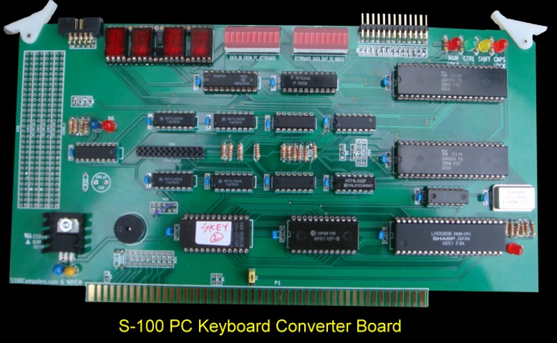
A Production S-100 Board.
Realizing that a number of people might want to utilize a board like this
(and the fact that I have 2 other S-100 systems that could use one) together
with Andrew Lynch at N8VEM (see
here) we have
just completed of laying out a "proper" commercial type S-100
board. Through Andrew's magic hands (and hard work) a very nice S-100 board
has emerged. Here is a picture of the board. If
you have an interest in such a bare board, let Andrew or I know. This
clearly applies only to people who know what they are doing and can do
a little soldering and board assembly. There would be little hand holding
at this stage.
Future Use Of The Board
The board has great potential for many applications. Because the key scan
codes are processed and translated using a Z80 it is easy for anybody
to take my KEY-DIAG.Z80 code (see below) and adapt it for their own specific
application and test it under CP/M. Things like buffering whole lines
of character input before sending it to the computer with a CR, or
program specific character lookup tables to control the screen cursor in
special ways are two simple examples that come to mind, or convert function
keys into special character strings for common commands for special
programs.
The board has multiple jumpers for allowing users to have much more control
on the system. These are not currently implement but you can use all of the
PIO status signals with software if needed. These are brought up to the P55
connector. There is the ability to trigger any of the S-100 interrupt
lines and in fact the ability to communicate back to PC keyboard (see
jumpers P68 and p69).
Building The Board.
For people that are interested in building this board here are some comments
and step by step instructions. First install
the voltage regulator, capacitors and IC sockets. You have a choice of
using the HP 5082-7340 hex displays or the LED bar displays (or both).
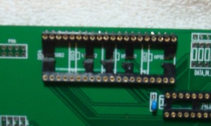
If you are using the HP hex display you need to arrange a special socket for
this board. Take a 40 IC socket and cut it in two so the spacing is as shown
in the picture below. Insert the (costly) HEX displays carefully. Note
the position of pin one on each chip and where it is on the board. Left to
right there is a one pin spacing, two pins, and then one pin spacing.
Make sure you jumper the S-100 Reset (or better) slave clear connection to
the S-100 bus.
Insert the board in the S-100 bus and check that +5 volts is getting to each
socket. Now install only the 4MHZ oscillator, IC5 (74LS06) U6
(74LS32), and the Z80. Do not connect up any jumpers etc. yet. Burn a
2716 EPROM with just 76H in every position in it and insert it in the ROM
socket (U8). Turn on the power. The LED at the bottom of the board
should come on indicating the Z80 has read the EPROM correctly. Do not go
further until you see this result. If the "Halt" LED does not come on you
may have a bad chip and/or solder connection.
If all is OK then install the two
PIO's and the RAM chip (U9, a 2KX8 6116). Repeat the above test.
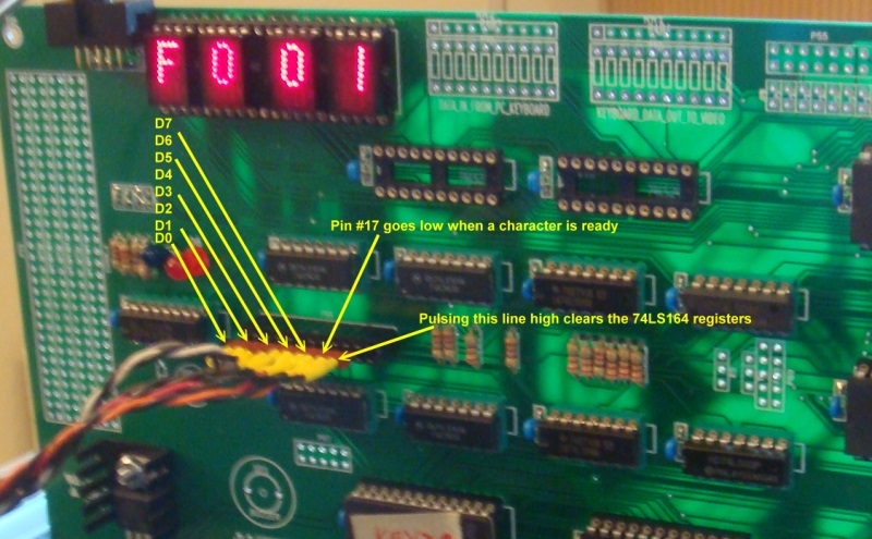
You now have a working Z80/ROM system! Next install all the IC's except the
Zenier diode D8 and R40 and the bell/buzzer circuitry (74LS123).
On the back of the board we have to make a few small corrections.
Connect a wire between pin 3 of U13 (74LS123) and +5V. Cut the trace coming
from the IBM keyboard data line going to U13 pin 13 and connect the data
line to U13 pin 4. (This has the effect of having the LED flash on when a
character comes in, rather than normally being on and going off when a
scan code is received. You can leave it as is if you like). Connect a
wire between the + terminal of the buzzer and +5 volts. Lastly, but very
important pin 17 of both PIO's must not float. They go to the P55 connector
but normally are not connected to a keyboard. At P55 jumper both pins
to ground . This is absolutely essential for this board to function
reliably. A floating input will cause the board to randomly lock up.
See the picture below which illustrates these jumpers.
Before you use the board you need to setup a number of board jumpers for
your particular hardware configuration.
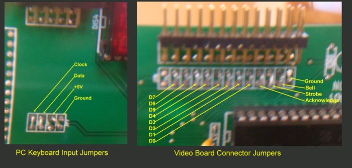
First the PC Keyboard In socket connection. This 10 pin socket is at the top
left of the board. Only the bottom 4 out of the 5 bottom row of pins
are used. They are Ground, +5Volts (to the keyboard), and the clock and data
signals from the keyboard. Below this socket is a set of jumper positions to
allow you to match up any socket connection you may have with what this
board needs. The signals must be as follows:-
You can jumper the wires on the front and back of the board if they must
cross. Please be absolutely sure you send the correct +5Volts and
ground to the correct pins on your keyboard. See the diagram above at the
start of this article. It shows
the male pins of the keyboard socket at the end of the cable as you look
into it.
Next we need to collect the output ASCII data lines in a format that your
parallel video board recognizes. Since they are many possible formats
for the different S-100 video boards, the connection to these boards via the
top right connector goes through a series of jumpers. You will minimally
need to determine which lines are for data bits 0-8 of your keyboard input.
Also you will need a strobe line. Depending on your video board the strobe
can be a positive or negative going pulse. Jumper K4 with a short wire
bridge to suite your video board keyboard input. The output from PIO#2 pin
14 is normally low, pulsing high when a character is sent. On my
SD Systems 8024 Video board the strobe should be high to low so I run
the signal through the inverter IC6D (74LS06).
Some slow video keyboards may require the board to wait for an acknowledge
signal indicating it received the character and is now ready for the next
one. IF your board requires this (i.e. you cannot flood the system),
jumper K5 to recognize a positive or negative strobe signal. The
software PROM example I have below has this requirement commented out. If
you need it, you need to include that code. The reason I did it this way is
that not only do few video boards have this requirement but if the Ack
signal is not sent the software will hang waiting for the signal giving the
appearance the board is not working.
Ok, we are now ready for a functional system. First see if you can get the
board running without the need for diagnostic software (see below).
Download the SKEY.Z80 code, assemble it to a hex file and burn it into a
2716 EPROM. I have used old 350ns EPROMS with a 4MH Z80 on this board.
I have run it up to 5MHz with no problems, so the simple logic and timing on
the board should be no problem with standard 2716 EPROMS.
Insert the board into your system with the keyboard in and out connections
as described above and power up. The board should display 13 in the Keyboard Out display. This
indicates the board ran through its diagnostic test OK and is ready to work.
See the software for error codes. If working correctly
whatever you type no matter how fast you type the board should keep up. For
example pressing the "1" key should display 16 & 31 on the In and Out
displays. If you do not see this go to the diagnostic section below.
The final thing we need to do is activate the "bell" function. You may
not want this but if your S-100 video board sends out a signal that the
ASCII 07H has been received it can be user to sound a bell/buzzer.
This goes back to the old teletype days. Having the ability to ring a
bell is nice. The problem is different S-100 board manufactures used
different signals to do this. They would either pulse high or low for a
fraction of a second where a buzzer in hardware was expected to generate its
own sound, remain high/low for a length of time, or actually generate the
high/low tone signal themselves in software. The bell circuitry on
this board should allow most formats to work by selecting the appropriate
jumpers on P67. The one complication of using the direct
high/low level approach is the bell sounds if the P55 connector is
disconnected from the board. This can be annoying. I use the low to high
transition triggered signal approach with the 74LS123 with my SD Systems
8024 Video board. This way whenever the P55 connector pin 23 goes
from low to high the bell will sound. Changing the values of C20 and
R33 will vary the length of time. Anything between 47 and 100uF seem fine.
Do NOT use the resistor Zenier diode circuit to power the buzzer. Ther was
an error in the design. Going above 5 volts casues the buzzer to stay on.
Buzzers like the Jameco #76065 work fine at 5 volts.
Here is a short video demonstration of the board in action. Random keys are
struck on the keyboard. The left most pair of HEX displays shows the
arriving scan code. The right pair shows the corresponding ASCII character
sent to the computer.
Diagnostic Software. In theory you should not need any of this, but just in case you run into
problems I have written a few very simple programs to help identify the
problem. Much depends on the nature of the problem. Assuming your
board passed the above "Halt" test. The next question is do you see 12 on
the data out Hex or LED display? The SKEY.Z80 code after initializing the
PIO's, first fills the 2K of RAM with 0's it then checks that's the case.
If there is a RAM problem the output code will be 10H. Check hardware.
If the Z80 somehow jumps to non-existent RAM/ROM it will see 0FFH on the
data lines causing it to jump to 38H in the ROM which will put 38H on the
display. Again a hardware issue.
Check the PIO's are working correctly.
This is a simple loop test. We first input from PIO#1 and output the
value to PIO#2. The values then increase by 1 each time in a loop on the
output display. You can see Key-DIAG(PIO-Test1).Z80
here. See above, for
the source code itself.
This is a slight variation. We first input from PIO#1 and output to
PIO#2 continuously. There may be problems with the 74SL164's (see below)
but whatever appears on the input display should appear exactly the same on
the output display. Note neither of these programs requires RAM. You
can see Key-DIAG(PIO-Test2).Z80
here. See above, for
the source code itself.
Using the Diagnostic Connector Port The board has actually two distinct hardware
sections. It really helps if you can establish where the problem lies.
Is it in the signal processing section or the Z80 translation section. The
first section of the board takes the raw clock and data serial data and runs
it through the four 74LS164's. The resulting scan code is presented
the Data IN Display and on pins 1-15 of the P66 "test Connector". Pin
17 on the test connector will go low as well. Normally this same
signal is see by the Z80 via pin 27 of PIO #2 (indicating a complete scan
code is in). The Z80 then sends out a clear signal to the 74LS164's via pin
15 of PIO#2 for the next scan code. What we do is remove PIO#2, bend
out pin 15 and reinsert the chip. We will control this line ourselves with a
separate connection.
To do this you need to have your current S-100 system working (without this
board for actual keyboard input) or use another computer . You will need to
have two parallel input ports and one parallel output ports. You will see in
the software (see below) I use the following equates. If you are using
a separate computer/ports to control this S-100 board be sure to use a
common ground line (P66 connector pin 23).
KEYOUT EQU 01H
;Data port for direct output to SD Systems video board
KEYIN EQU 04H
;Raw data port for IMB keyboard (Diagnostic port)
KEYCLEAR EQU 07H ;Pulsing bit 0 high
clears 74LS161 Shift Regs
KEYSTAT EQU 07H ;Input bit 0
is zero if IBMPC Key char ready
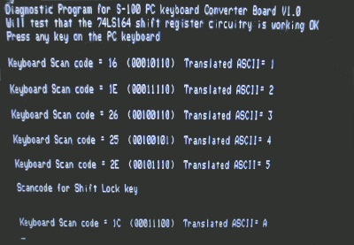
Download the program
SKEY-DIAG.Z80 from here. Set the equates to your
system and assemble it. Run this CPM program. It is the exact same
EPROM code used to run your board except it is surrounded (front & back)
with diagnostic code. When you send a scan code to the board the program
will show you what it got going in and what is getting translated for output.
The input values should show up on the input HEX/LED display however the
Output display will not. Instead it will appear of your Computer screen.
Here is an example:-
This should help you track down any hardware/software problems you have with
the board.
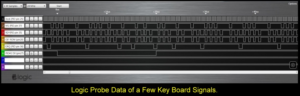
Also a good Logic probe can help. Here is a sample of a few key signals.
Improving the EPROM Software.
If you wish to add more software functions to the EPROM based software
rather that burning 2716 EPROMS each time for debugging you can modify the
above diagnostic code (make sure the DEBUG equate = TRUE) check it out with
the board itself under CPM as described above and when it is perfect set the
DEBUG equate to FALSE and reassemble the ROM only code with the ORG at 0H.
If you have suggestions, comments or updates for this board please do so
using the Forum section of this web site .
A Production S-100 Board.
Realizing that a number of people might want to utilize a board like this
together
with Andrew Lynch at N8VEM (see
here) we have
completed a second run of these boards. We will collect names for a third
batch if needed. If
you have an interest in such a bare board, let Andrew know via e-mail at:-
lynchaj@yahoo.com Please note all the above
clearly applies only to people who know what they are doing and can do
a little soldering and board assembly. There will be little hand holding
at this stage.

.jpg)